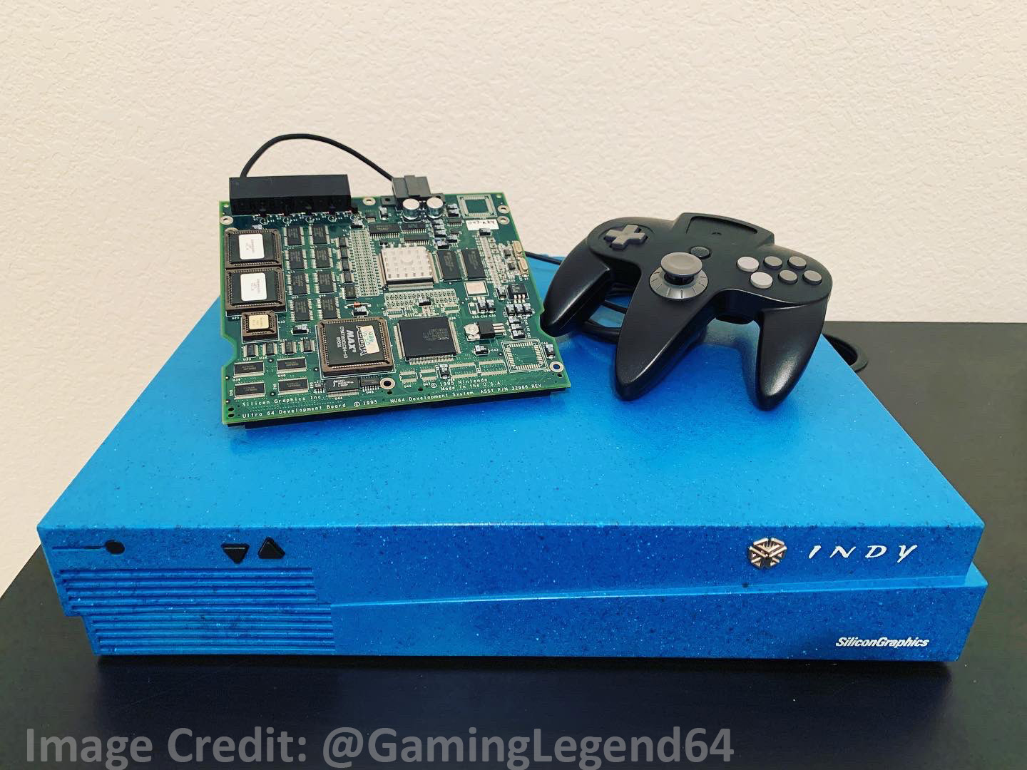
Shown below is the one and only… Ultra64 Development Board (Rev 2.0).

The Ultra64 Development board was a proprietary GPIO board for use with a Silicon Graphics Indy workstation.

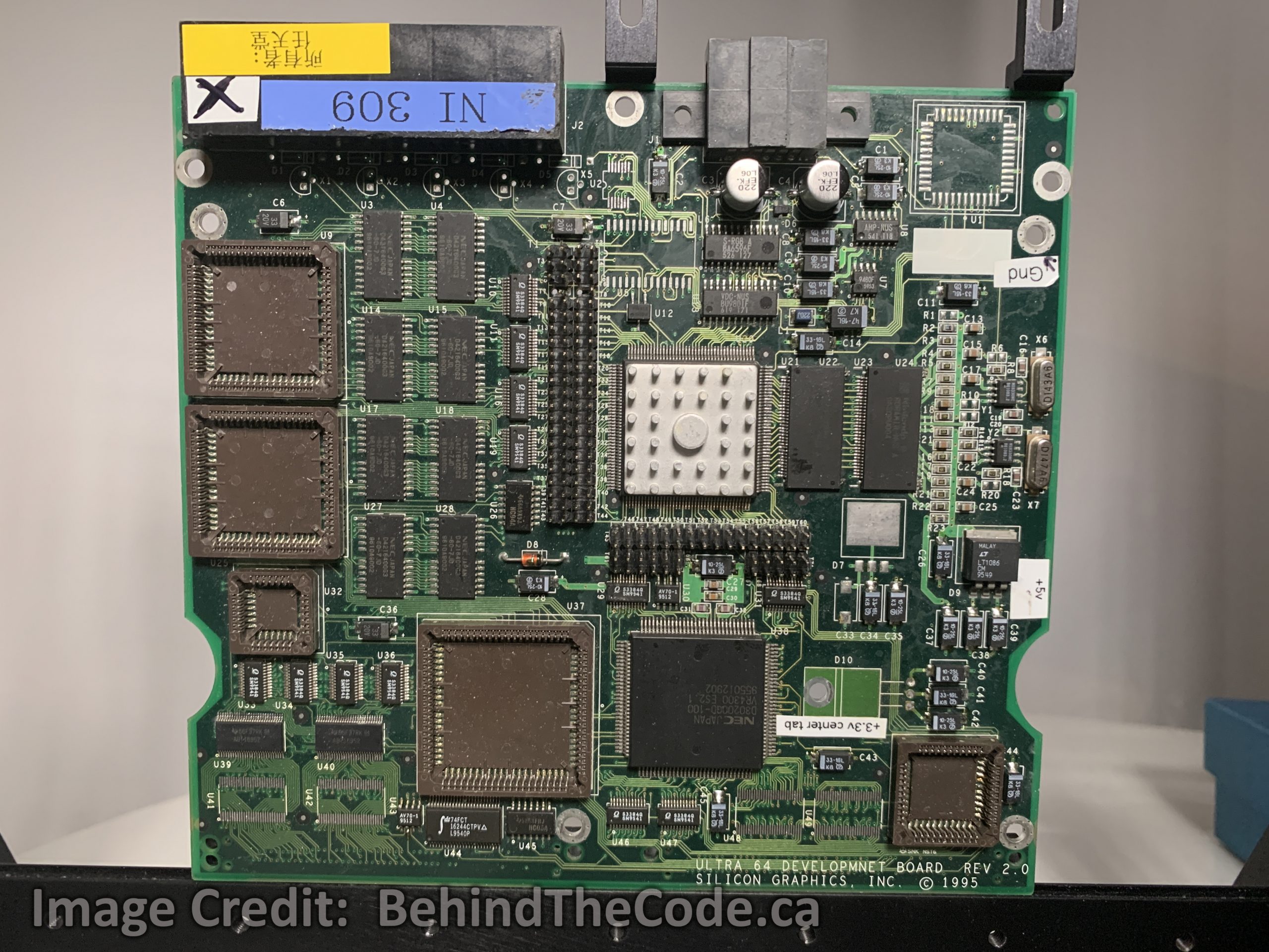
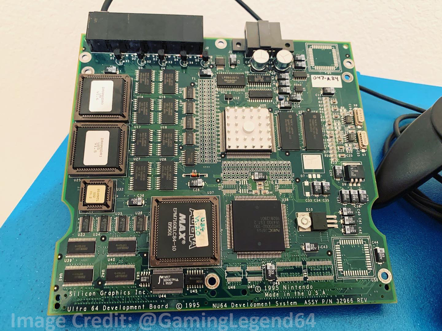
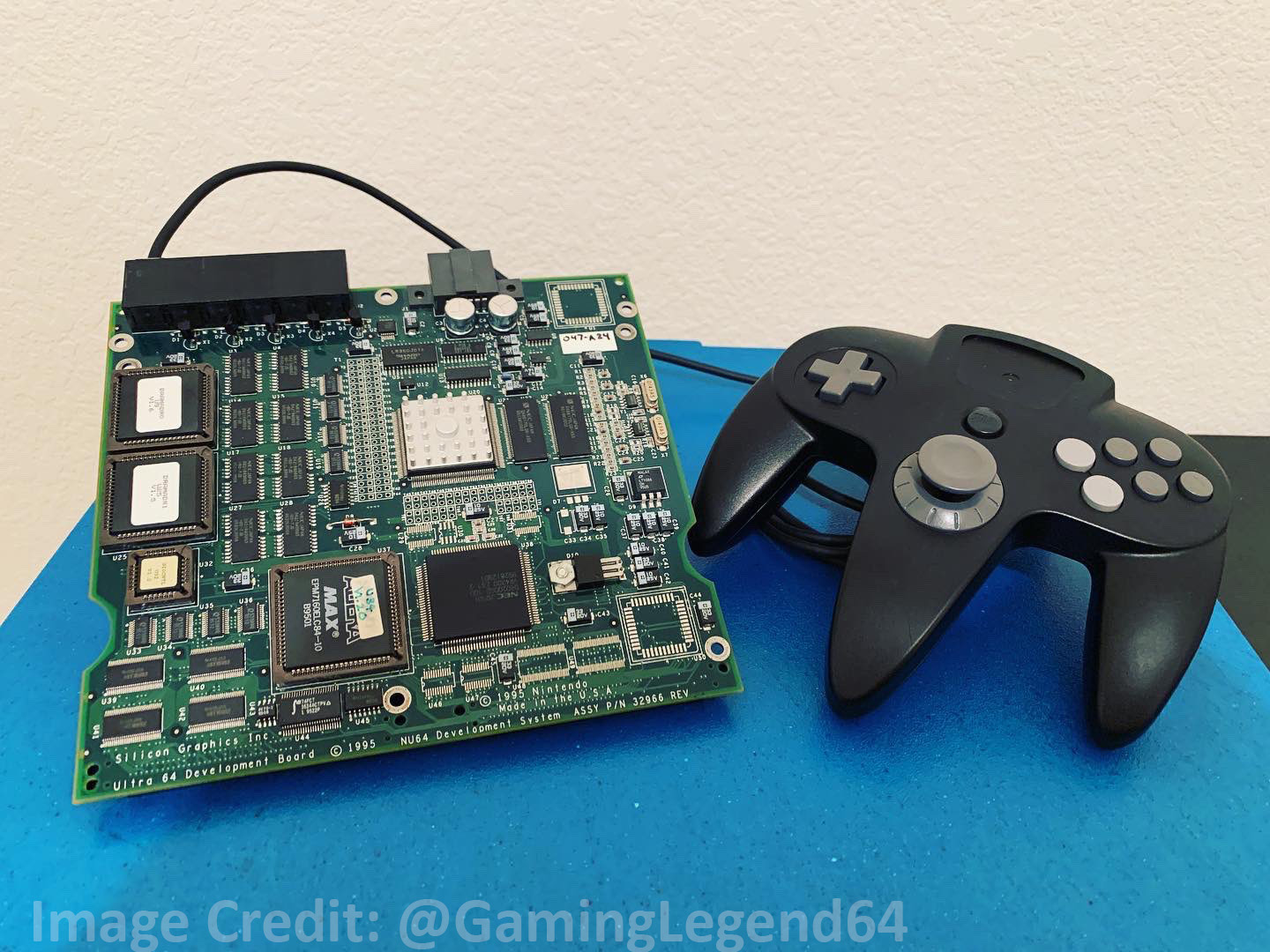
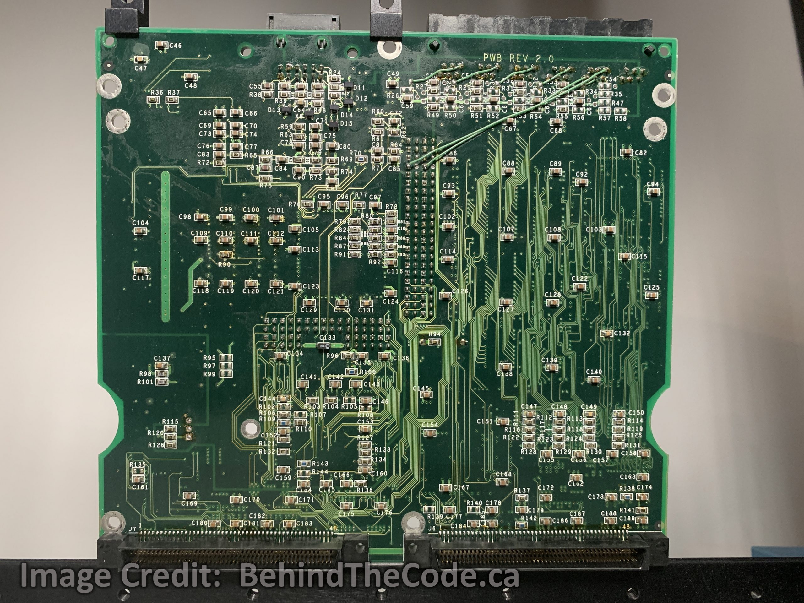
The most common board used was the Revision 2.0 model. Designed and built by Nintendo and Silicon Graphics (SGI) for programming and debugging N64 games. This was one the first debuggers available to N64 developers. As shown below:
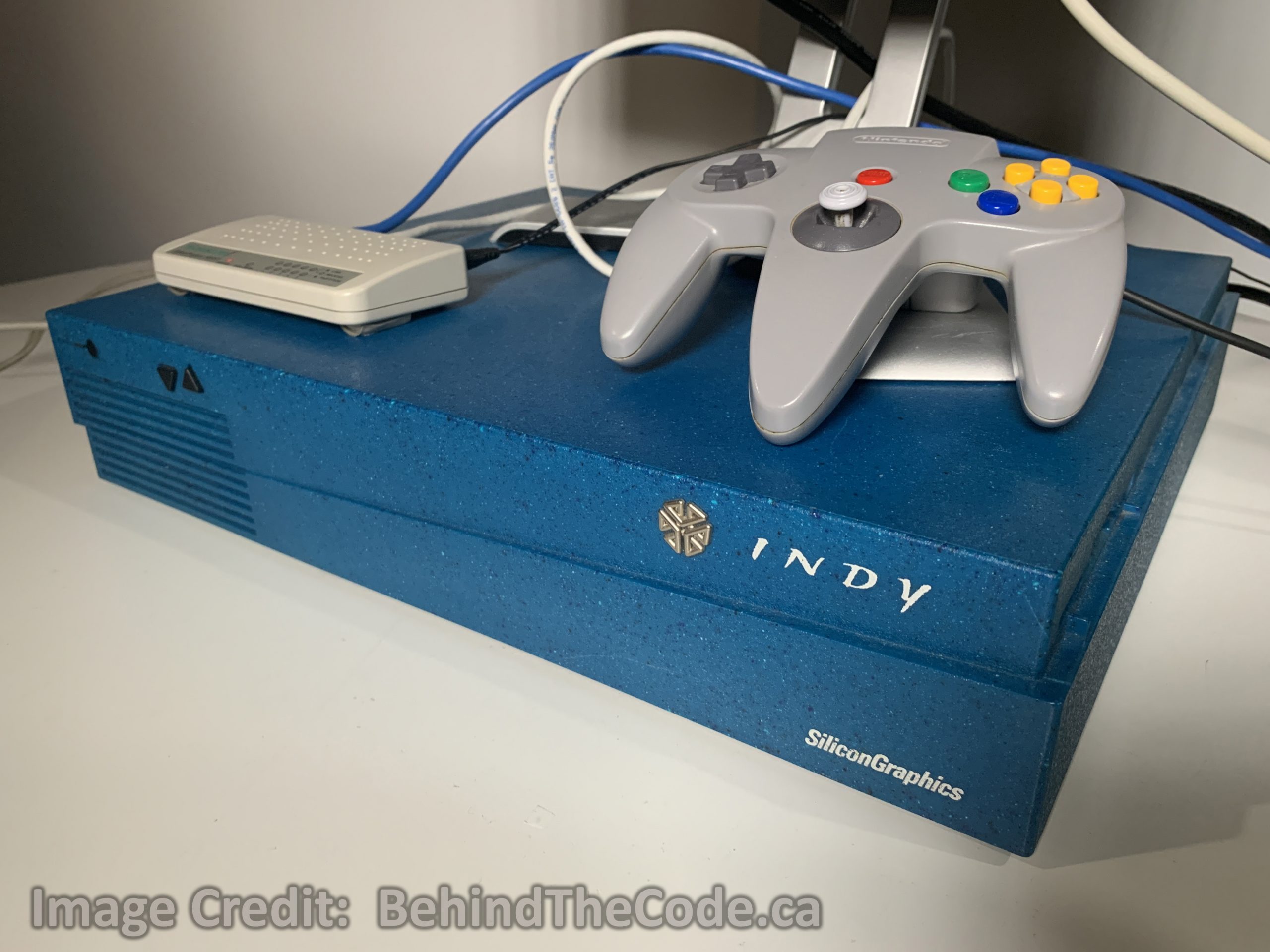
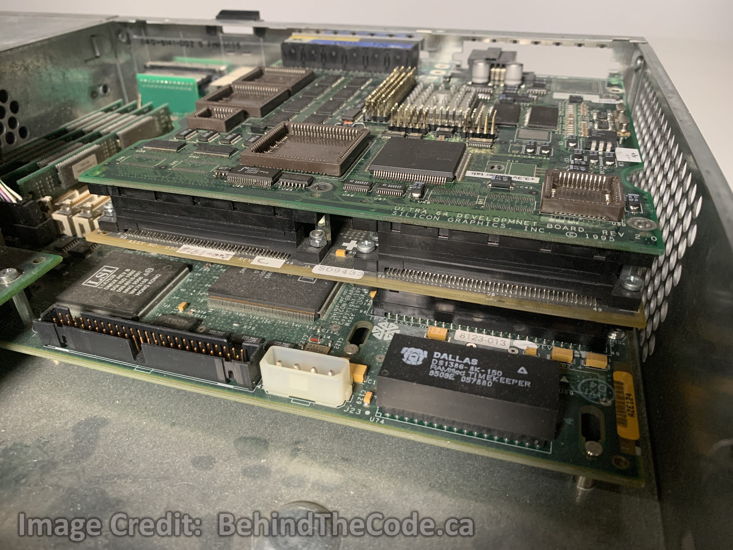
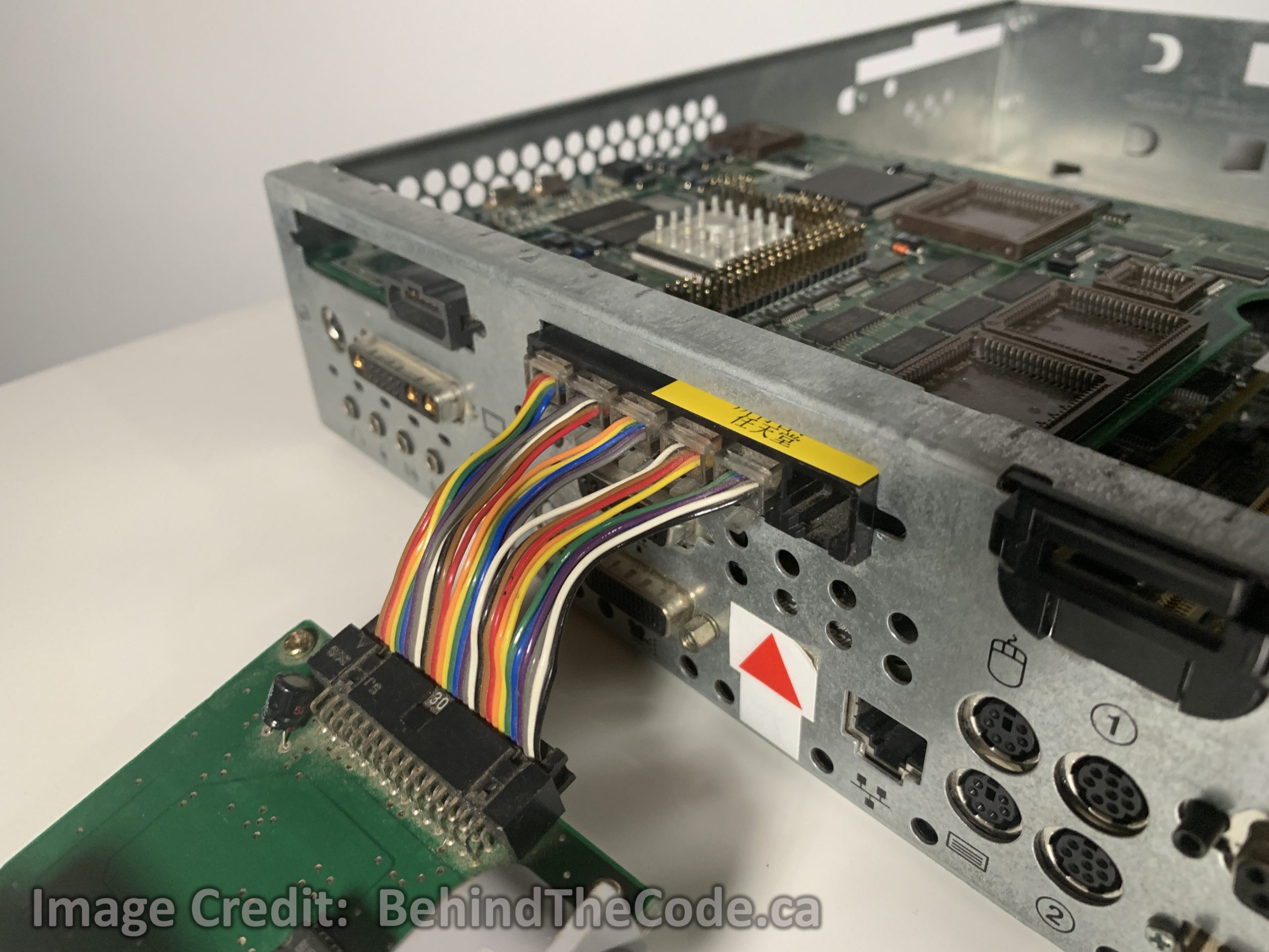
This GPIO board was to be installed in an INDY Workstation.
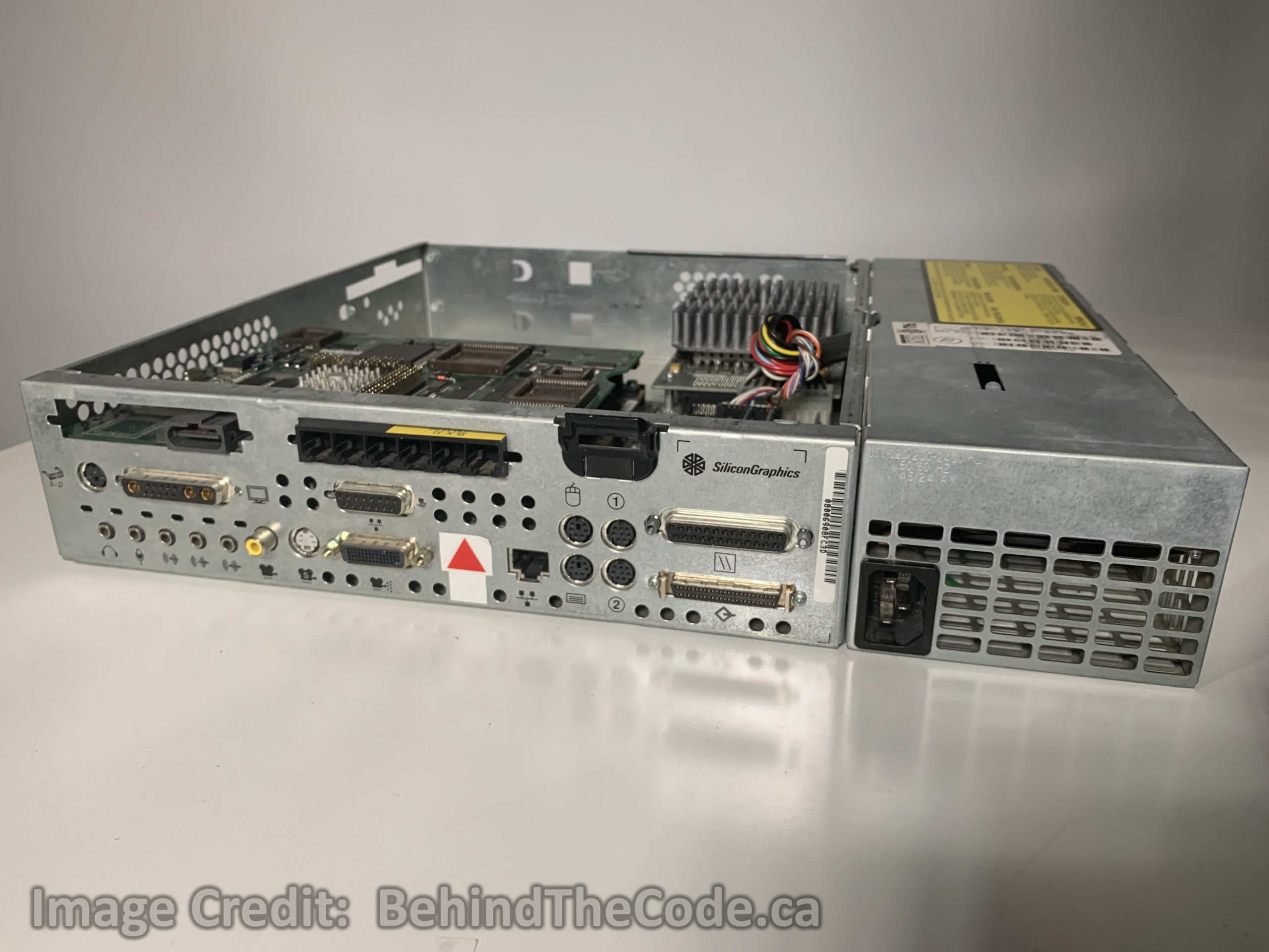
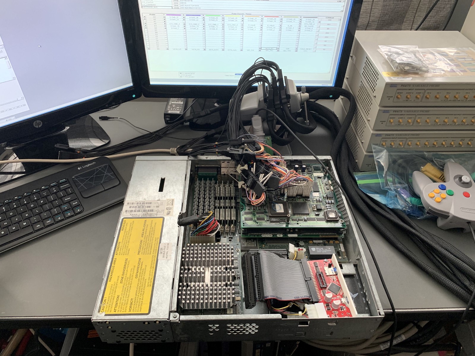
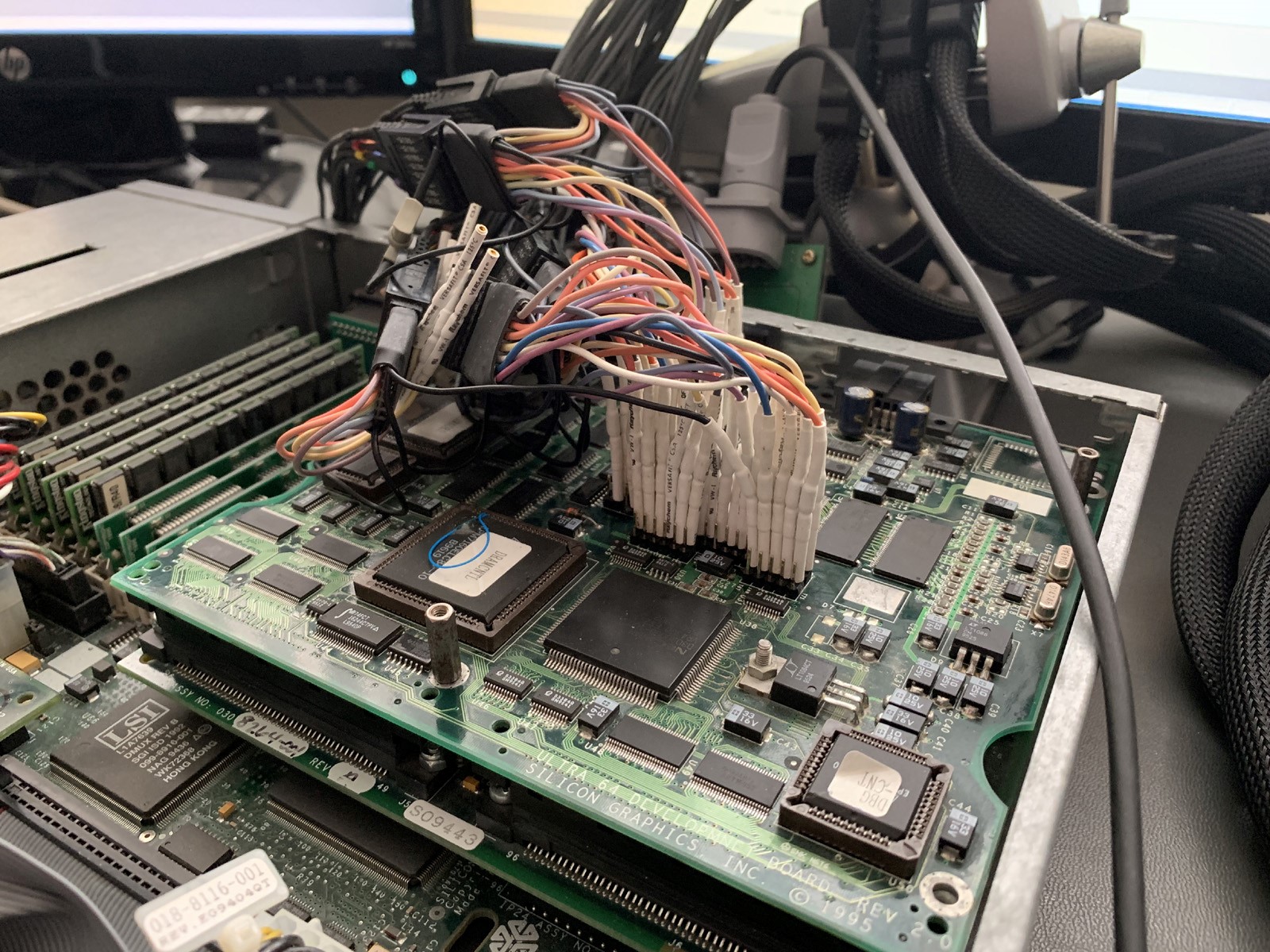
As shown, the Ultra64 Dev board mates to the Indy GFX board by connecting to the two bottom I/O ports.
The boards Audio/Video output and RJ-11 ports are accessible on the back side of the Indy. Using a Standard Nintendo Multi Video cable, developers could connect a color video monitor, or they could also feed the composite video signal to the Indy’s video input connector. (Yellow RCA jack) This allows the Ultra64 video to be displayed on the Indy desktop screen for previewing. As shown further below. (Picture-in-Picture)
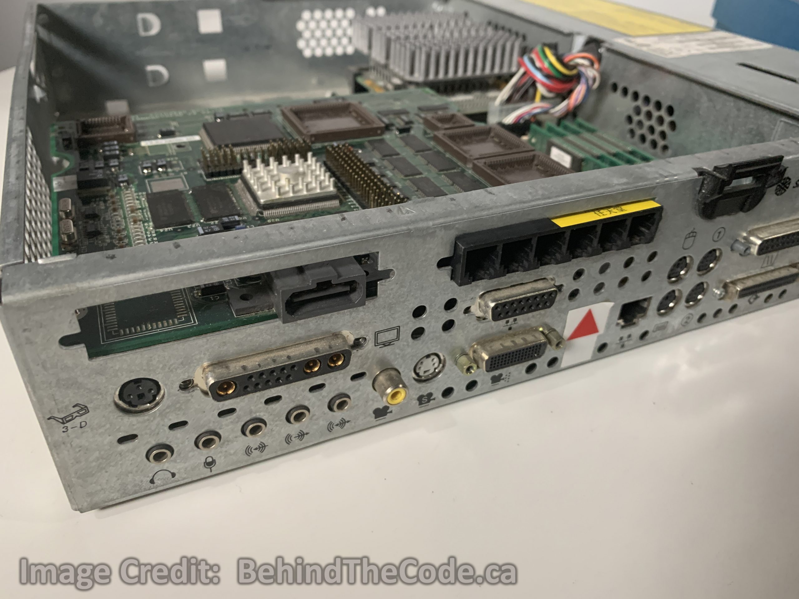
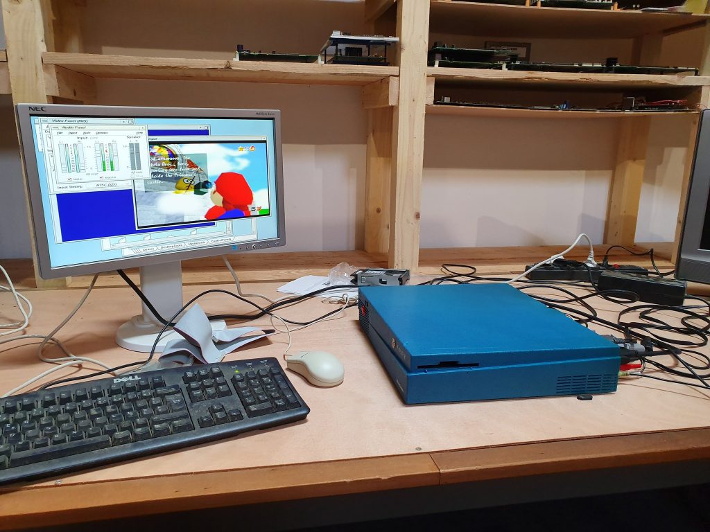
Image credit @ben1040 (PIX BEN on Twitter)
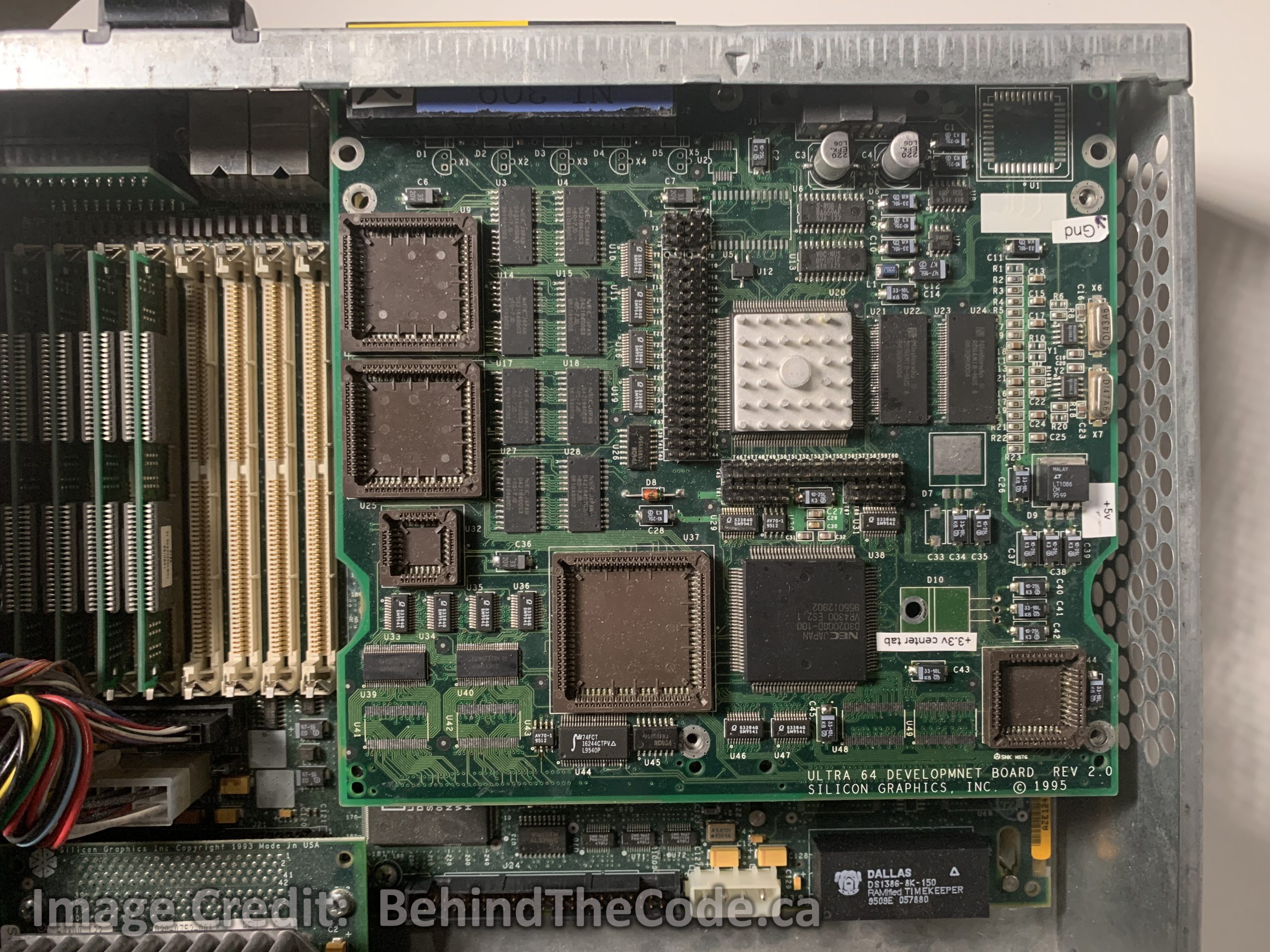
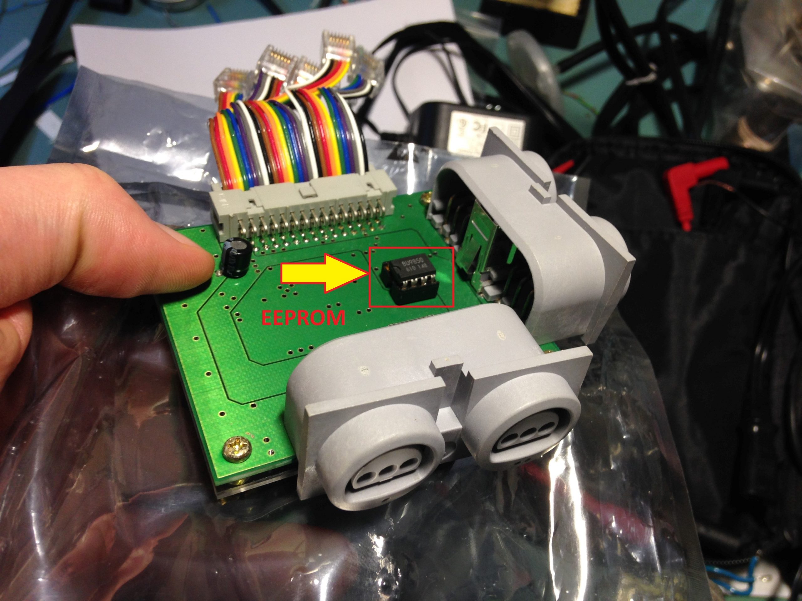
The RJ-11 ports on the Dev board were for a special adapter board called the JOYBUS board. This adapter allowed you to connect up to (x4) N64 controllers. The Joybus board also houses an EEPROM chip for development use and testing. (Save game data)
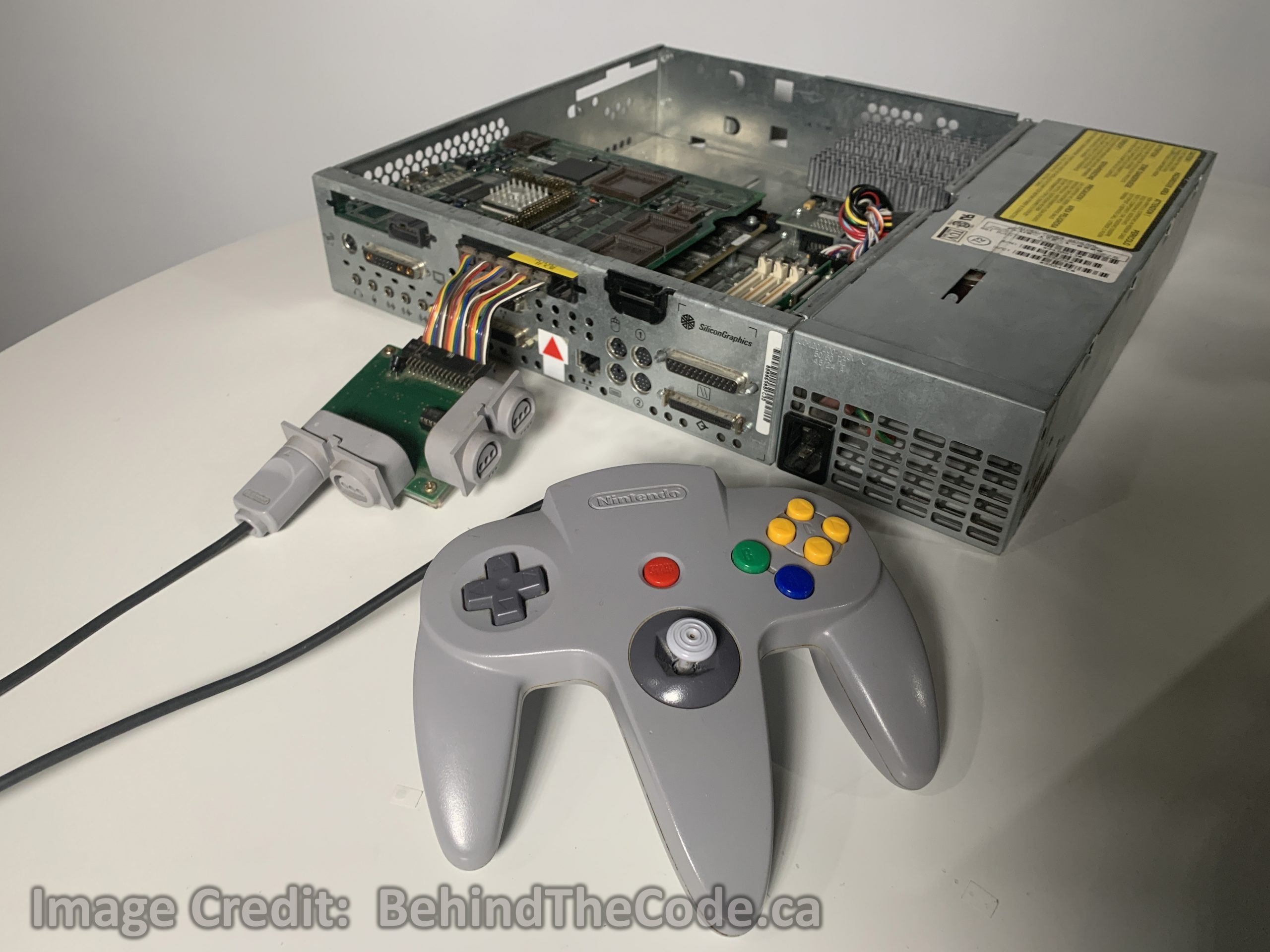
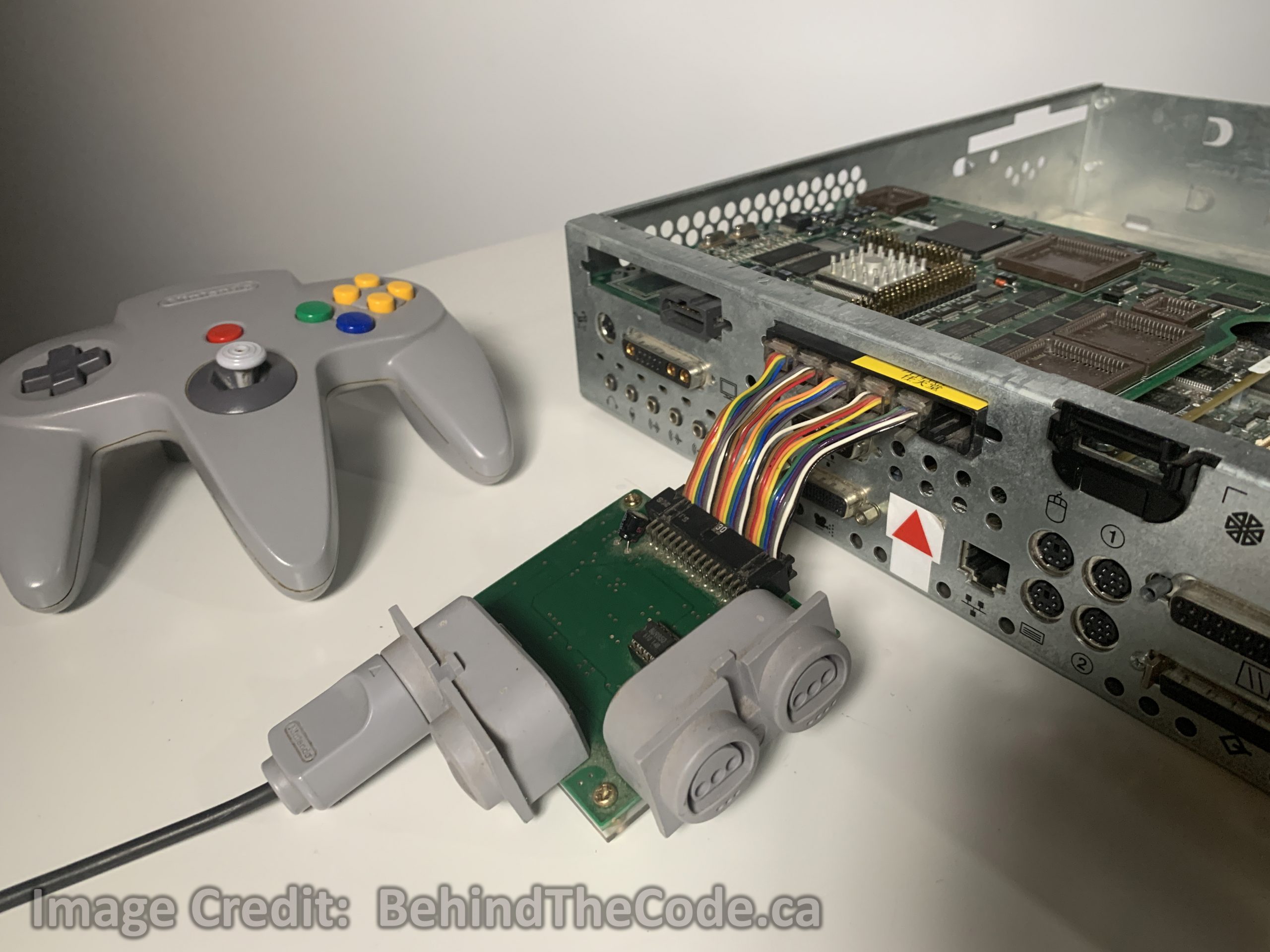
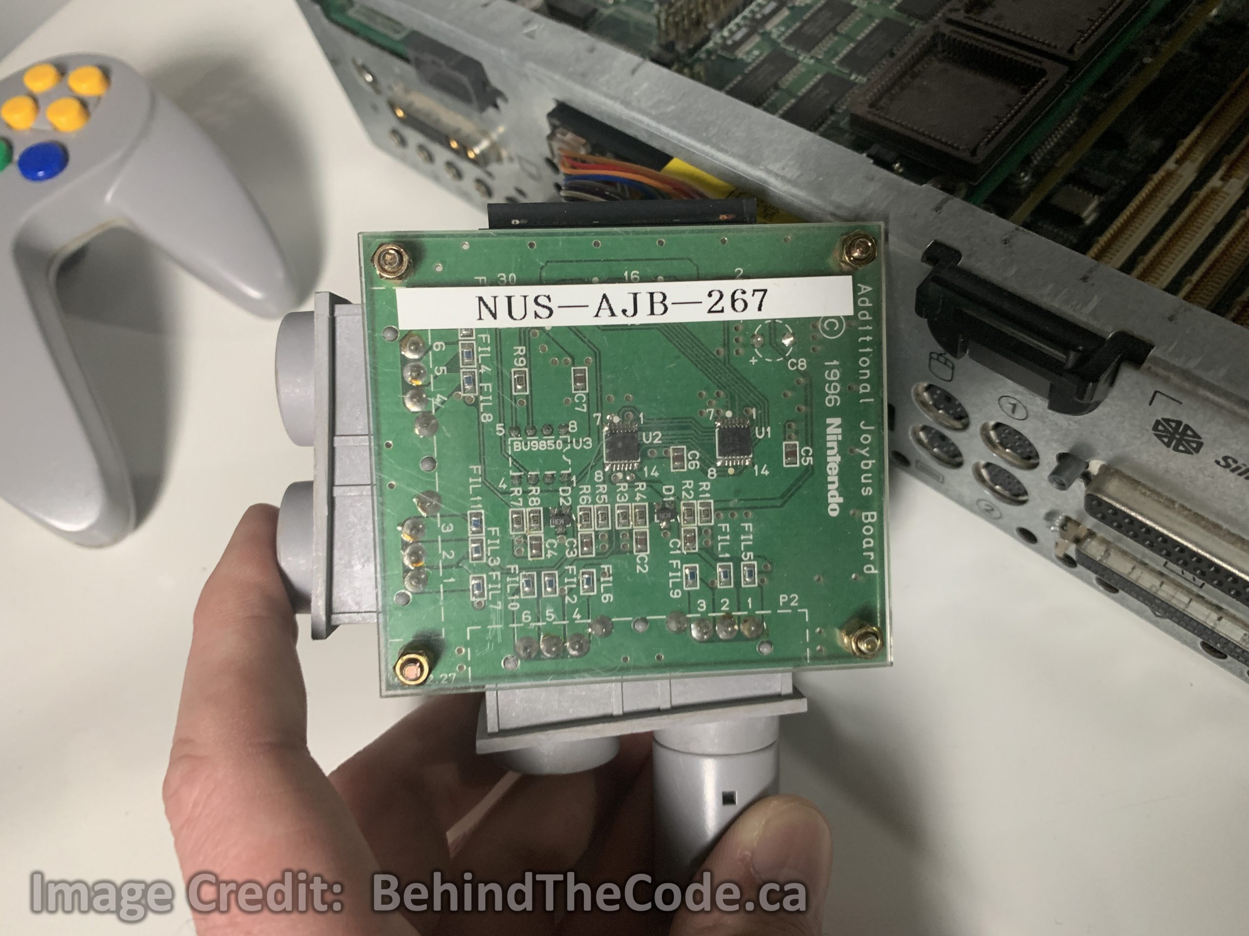
Notice that the 6th RJ-11 port is not used. Ports 1-4 are for the N64 Controller interface signals, and the 5th port is for routing the EEPROM data signals. (This unit needs a good cleaning wouldn’t you agree!!)
Shown below is the back side of the JOYBUS Board. There are several passive components and Logic conditioning chips in place to stabilize the digital signals being sent to and from the Dev board.
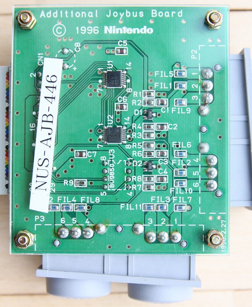
The RJ-11 Port#5 is used to pass signals to and from the Joybus boards EEPROM chip. As shown in the photo below, the PIF chip (U5) routes a “COLDRESET” and clock signal “SEC_CLK” to RJ-11 port#5 using AWG30 Tie-line/Bridge wires. Clearly seen on the back of the Dev board PCBA.


You can also see how RJ-11 port#6 is unused…with no PCBA traces in place.
The PIF chip has x6 controller channels.
- CH 1-4 = Controllers
- CH 5 = EEPROM
- CH 6 = GPIO for CPU’s Pre-NMI interrupt.
Ultra64 Development Board Rev 1.0
Here is an Extremely rare version of the Ultra64 dev board. The Rev 1.0 model.
This version of the board was used to debug some of the very first N64 games. What’s also interesting is the kit did not come with a Joybus adapter board. It used a very early version N64 controller. As shown in the images below…make note of the controller Analog stick. It is much larger than the retail versions sold with standard N64 consoles.
These “Ultra64” controllers were black in color and the end cable was outfitted with an RJ-11 connector. It would connect directly into the Ultra64 dev board RJ socket.
Images Provided by @GamingLegend64 (Twitter)